Programming Jig User Guide
User Guide. Release 1.0
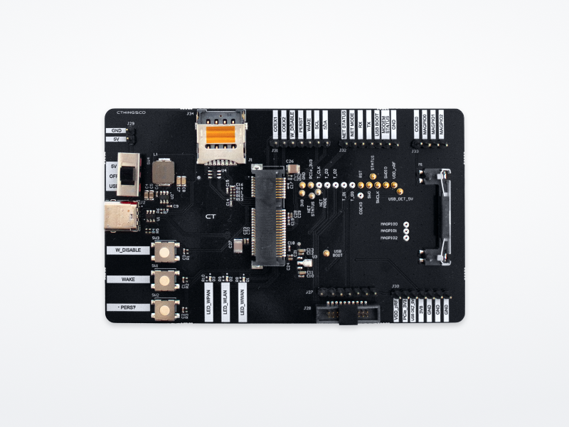
Develop and debug your own Connectivity Card firmware!
CTHINGS.CO offers a range of Connectivity Cards with various software options, but we understand that some projects may require even more flexibility. To make our Connectivity Cards even more versatile, we now offer M.2 and mini PCIe programming JIGs, designed to expand your capabilities and streamline your workflow.
CTHINGS.CO Programming JIGs offer two key functionalities: They provide a seamless programming experience with a built-in J-Link/J-Trace connector and SWD signals routed to 100-mil headers. Once programming is complete, all essential signals from the M.2 / mini PCIe edge connectors are accessible via the headers. Plus, with USB routed to a USB-C connector, you can start testing your software immediately after programming.
Description Mini PCIe Jig
Introduction
Mini PCIe jig offers USB that can be used to power the mini PCIe card and pass the USB signals from PC to the card. That way after programming the card can be immediately evaluated. Testing automation is also possible. If measuring the power usage is desired there is also an option to provide external 5V supply to the headers on left-top corner. Slide switch let’s you select the power source. All low-speed signals that are present on the mini PCIe connector (so no PCIe lines) are routed out to the 100 mil header on top of the jig. That way it’s easy to interact with the card while developing the firmware. Power supply rails and programming connectors are located on the bottom of the PCB. There are 3 LED signals specified in the mini PCIe specs. The LEDs are available on the jig as well; labeled LPWAN, WLAN and WWAN. The most important signals like RESET, WAKE and W_DISABLE are available both as goldpin headers and buttons, so user can easily simulate W_DISABLE, WAKE and RESET states. The JIG also has a SIM card slot allowing user to evaluate modem operation after flashing the firmware.
Usage
Programming
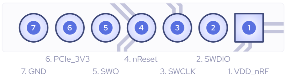
To program the card, you need to connect power supply and programmer. Each of those can be achieved in different ways. Power can be delivered to 5V HDR or through USB-C connector. Remember to select corresponding position of the power selection switch. Programmer can be connected either using 20 pin 50 mil J-Trace connector or using headers above it. Pinout of the headers is shown below:
Note
Pin 1 is the target VTref; pin 6 is the supply voltage of the card.
After connecting the power supply and programmer, insert the card into the mini PCIe slot and push it into the lock. The card is now ready for programming.
Debugging / testing
Setup of the card should be identical to the one described in the programming section. Feel free to use any of the available signals, buttons and LEDs.
Pinout specification
Signals available on headers
COEX1
COEX2
W_DISABLE (also available as a button)
PERST (also available as a button)
WAKE (also available as a button)
SCL
SDA
Card-specific signals available on headers
NET STATUS (combo card)
NET MODE (combo card)
UART (RX and TX) (combo card)
USB BOOT (combo card) — for EG25 firmware recovery
COEX0 (nRF9161 card)
Power supply rails available on headers
mini PCIe supply 3V3 rail monitoring
3V8 for EG25 supply (combo card)
1V8 for nRF52 (nRF52 card)
Status LEDs
WPAN
WLAN
WWAN
Variants description
Two variants of mPCIe programming jigs are available:
for LTE and nRF COMBO cards
for other CTHINGS.CO Connectivity Cards
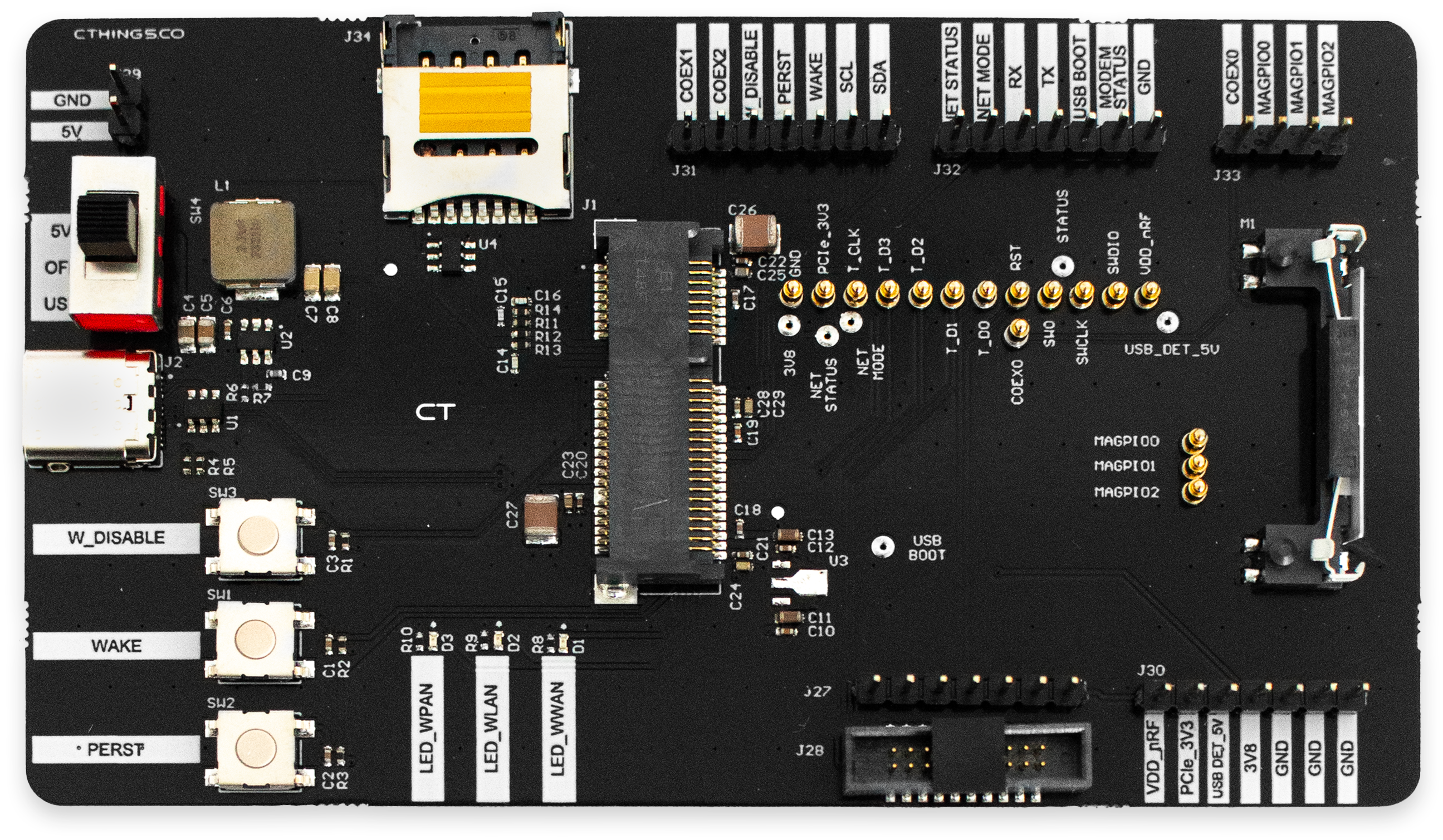
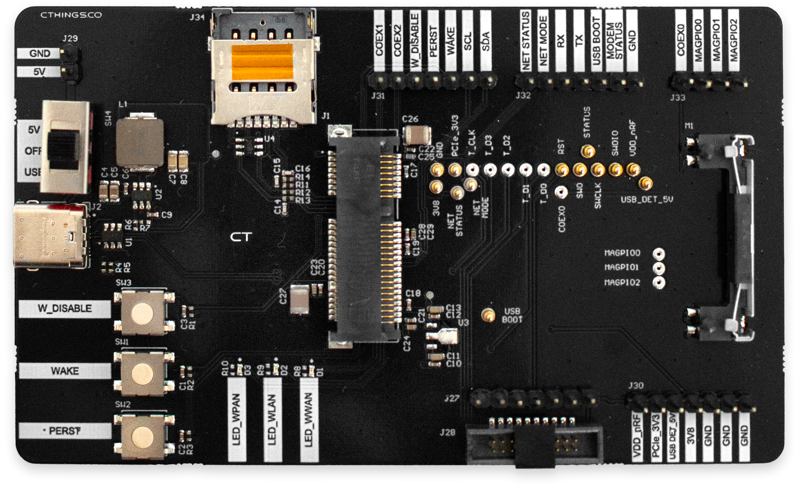
The only difference between the versions is which pogo-pins are mounted. Because we have different Connectivity Cards there are multiple layouts of test-points on the bottom of the cards. Some pogo-pins would be too close to each other to be mounted. Also COMBO card has elements on the bottom that would collide with pogo-pins for different cards.
mPCIe_jig standard
mPCIe_jig for mPCIe_LTE_and_nRF
List of compatible cards with each variant:
mPCIe_jig standard |
mPCIe_jig for mPCIe_LTE_and_nRF |
|---|---|
mPCIe_NRF9160_FLASH |
mPCIe_LTE_and_nRF |
mPCIe_NRF9160 |
|
mPCIe_NRF |
|
mPCIe_MGM240P |
Description M.2 Jig
Introduction
M.2 jig offers USB that can be used to power the M.2 card and pass the USB signals from PC to the card. That way after programming the card can be immediately evaluated. Testing automation is also possible. If measuring the power usage is desired there is also an option to provide external 5V supply to the headers on left-top corner. Slide switch lets you select the power source. All low-speed signals that are present on the M.2 connector (so no PCIe lines) are routed out to the 100 mil header on top of the jig. That way it’s easy to interact with the card while developing the firmware. Power supply rails and programming connectors are located on the bottom of the PCB. There are 2 LED signals specified in the M.2 specs. The LEDs are available on the jig as well labeled LED1 and LED2. The most important signals like reset and W_DISABLE are available both as goldpin headers and buttons, so user can easily simulate W_DISABLE, WAKE and RESET states.
Usage
To program the card you need to connect power supply and programmer. Each of those can be achieved in different ways. Power can be delivered to 5V HDR or through USB-C connector. Remember to select corresponding position of the power selection switch. Programmer can be connected either using 20 pin 50 mil J-Trace connector or using headers above it. Pinout of the headers is shown below:
Note
Pin 1 is target VTref; pin 6 is supply voltage of the card.
After the power and programmer are connected insert the card to the M.2 slot and screw it in. Now you can program the card.
Pinout specification
Signals available on headers
COEX1
COEX2
COEX3
VENDOR DEFINED 1 (pin 38)
VENDOR DEFINED 2 (pin 40)
VENDOR DEFINED 3 (pin 42)
W_DISABLE 1 (also available as a button)
W_DISABLE 2 (also available as a button)
PERST (also available as a button)
WAKE (also available as a button)
CLKREQ
SCL
SDA
ALERT# (marked as IRQ)
Power supply rails available on headers
mini PCIe supply 3V3 rail monitoring
AUX 5V rail (nRF52 card)
1V8 for nRF52 (nRF52 card)
Status LEDs
LED1
LED2
Reserved signals available on headers
Pin 36 (marked as CTS)
Pin 34 (marked as RTS)
Pin 32 (marked as RXD)
Pin 22 (marked as TXD)